
SEO excerpt: NVIDIA is investing $3.5 billion in MediaTek as the chipmakers expand NVLink Fusion across custom data-center accelerators, AI PCs and vehicles. The deal could shorten the path from custom silicon to rack-scale deployment, but pricing, customer designs and delivery dates remain undisclosed.
NEW DELHI, September 1, 2026, 5:00 p.m. IST — NVIDIA has invested $3.5 billion in convertible bonds issued by MediaTek and expanded a partnership that will put NVIDIA’s NVLink Fusion technology behind more custom AI accelerator designs, the companies announced Monday.
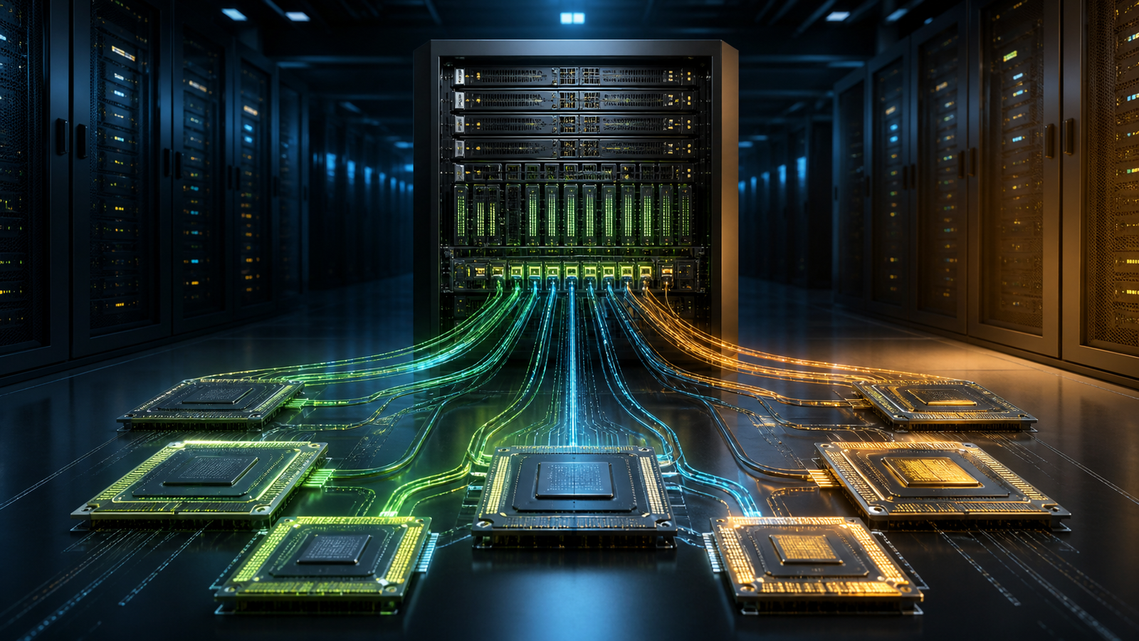
The agreement is notable less for another large AI-sector investment than for where NVIDIA is placing its technology. MediaTek will offer NVLink Fusion as a design foundation for custom XPUs that can connect to NVIDIA’s rack-scale systems. That gives cloud providers and model developers a route to build workload-specific chips without engineering every surrounding interconnect, memory, packaging and rack component independently.
For infrastructure teams, the development points toward a more heterogeneous AI data center: custom accelerators and NVIDIA GPUs could share elements of the same rack, network, cooling and management architecture. It may reduce integration work, but it also puts an NVIDIA-controlled fabric deeper into systems designed partly to reduce dependence on NVIDIA GPUs.
What NVIDIA and MediaTek confirmed
In their joint announcement, NVIDIA and MediaTek said the collaboration now spans three areas: custom AI infrastructure, local AI computing and automotive platforms.
At the data-center layer, MediaTek will use NVLink Fusion to help customers develop custom XPUs that connect to NVIDIA’s scale-up fabric and MGX rack architecture. The disclosed building blocks include an NVLink Fusion chiplet, NVLink-C2C connections between accelerators and compatible processors, and NVIDIA’s customized high-bandwidth memory technology, called NVHBM.
The companies said customers will be able to tailor connectivity, memory, packaging, performance and power characteristics to individual workloads. NVIDIA and MediaTek did not name customers, announce a production accelerator, provide a delivery schedule or disclose commercial terms for the design service.
The partnership also extends the companies’ work on multiple generations of NVIDIA RTX Spark and DGX Spark chips for PCs and developer systems, as well as platforms for software-defined vehicles. Those programs are separate from the custom data-center XPU effort and should not be read as evidence that one common chip will span all three markets.
The investment and the scrutiny around it
Reuters reported that NVIDIA’s $3.5 billion purchase forms most of MediaTek’s record $3.9 billion overseas convertible-bond offering. Reuters also reported that Alphabet participated in the offering, although MediaTek did not disclose the size of that investment.
The financing deepens NVIDIA’s financial ties to a company developing technology that can extend NVIDIA’s rack architecture. That has renewed questions about AI-sector financing in which capital providers also benefit from the resulting infrastructure demand. Reuters quoted an investment manager who distinguished this arrangement from directly financing a customer while still describing it as NVIDIA using its balance sheet to accelerate ecosystem growth.
That distinction matters. The announcement confirms an investment and a technology partnership, not purchases of NVIDIA GPUs by MediaTek or its future XPU customers. It also does not establish how much of the bond proceeds will fund NVLink Fusion products, when the bonds may convert to equity or what share of MediaTek NVIDIA could eventually own.
How NVLink Fusion changes the custom-chip path
A custom accelerator is only one part of an operational AI cluster. Teams must also qualify high-bandwidth memory, connect accelerators within a scale-up domain, design trays and racks, integrate power and liquid cooling, coordinate suppliers, validate distributed software and expose telemetry that operators can use during failures.
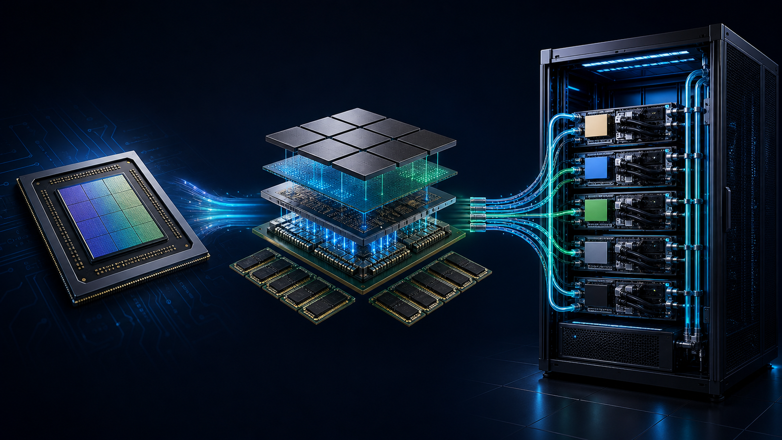
NVIDIA’s technical overview of NVLink Fusion presents the platform as a way to reuse those surrounding layers while allowing a customer-specific XPU to supply the differentiated compute. It says GPU and XPU systems can share rack footprints, networking, cooling, power delivery and management systems, which could let infrastructure planning begin before the final accelerator mix is fixed.
MediaTek adds custom-system-on-chip design, advanced packaging, interconnect and manufacturing expertise to that model. TechCrunch reported that MediaTek expects its custom data-center ASIC business to generate $2 billion in revenue in 2026, while noting that the company has not publicly identified its custom AI-chip customers.
The practical trade-off is architectural. A cloud provider can differentiate the accelerator and potentially tune it for inference, training or another workload, while relying on NVIDIA for more of the rack-scale foundation. That can shorten qualification work, but it may also make migration to a different interconnect or management stack more difficult later.
What platform and DevOps teams should watch
No immediate cloud instance, API endpoint or generally available accelerator was announced. Developers should not expect today’s SDK choices or model-serving prices to change because of the investment alone.
Platform teams evaluating future heterogeneous clusters should instead watch for operational evidence in five areas: which frameworks and model servers run unchanged; whether GPU and XPU telemetry uses consistent metrics; how workloads are scheduled and isolated across accelerator types; whether failed jobs can move to compatible capacity; and how firmware, drivers and distributed libraries are versioned across the rack.
NVIDIA says its software layer can include NCCL for distributed workloads, Dynamo and NIXL for disaggregated inference, and Mission Control for cluster management, telemetry and debugging. Those are vendor descriptions, not proof that a future MediaTek-designed XPU will support every component or provide feature parity with NVIDIA GPUs.
Procurement teams should also separate chip economics from system economics. A workload-specific XPU may lower cost for a narrow task, yet qualification, utilization, spare capacity, software maintenance and fallback paths determine the operating cost of the full service. GravityDevOps’ guide to LLMOps covers the lifecycle controls around production models, while its CI/CD tools comparison provides context for building repeatable validation and release gates around infrastructure changes.
What remains uncertain
NVIDIA has published performance and efficiency claims for NVLink and NVHBM, but no independently reproduced benchmark for a MediaTek customer XPU exists because no such product was announced. The companies also did not disclose pricing, named design wins, production volume, regional availability or a deployment timeline.
The confirmed news is therefore a strategic financing and platform agreement. Its technical significance will depend on whether customers ship custom accelerators through MediaTek, whether those systems interoperate as promised at rack scale, and whether the resulting operational savings outweigh deeper dependence on NVIDIA’s infrastructure stack.
For developers and operators, the next meaningful milestones will be concrete silicon specifications, supported software matrices, cloud availability and production measurements for throughput, latency, reliability and power. Until then, NVLink Fusion’s expanded reach is an important direction of travel, not a finished deployment.
Sources
NVIDIA and MediaTek’s joint partnership announcement; Reuters reporting on the bond investment; NVIDIA’s NVLink Fusion technical overview; and TechCrunch’s custom-chip market context.


